Radiation Damage in CCDs
used as Particle Detectors
C. J. S. Damerell
Rutherford Appleton Laboratory, Chilton, Didcot, OX11 0QX, England
February 1997
Introduction
CCDs sensitive to minimum-ionizing particles (hereafter referred to as
min-I particles) have found a niche as very high precision tracking devices,
used as vertex detectors for the detection of short-lived heavy flavor quarks or
 leptons, in high energy physics experiments [1-3]. As such, they must be
located as close as possible to the interaction point (usually starting within
10 or 20 mm). In this environment the capability of these pixel-based
devices to tolerate very high hit densities (typically
leptons, in high energy physics experiments [1-3]. As such, they must be
located as close as possible to the interaction point (usually starting within
10 or 20 mm). In this environment the capability of these pixel-based
devices to tolerate very high hit densities (typically
 )
is an important attribute. However, this environment may be quite demanding as
regards radiation hardness, a situation also encountered by users of imaging
CCDs in industry (nuclear, X-ray and electron microscopy, for example), for
space-based optical and X-ray telescopes, etc. Radiation damage in these
complex silicon devices is therefore relevant to numerous application areas and
has been studied for many years [4-16]. Reference [11] provides a particularly
valuable review. Despite being 17 years old, it remains the most comprehensive
general paper on this subject.
)
is an important attribute. However, this environment may be quite demanding as
regards radiation hardness, a situation also encountered by users of imaging
CCDs in industry (nuclear, X-ray and electron microscopy, for example), for
space-based optical and X-ray telescopes, etc. Radiation damage in these
complex silicon devices is therefore relevant to numerous application areas and
has been studied for many years [4-16]. Reference [11] provides a particularly
valuable review. Despite being 17 years old, it remains the most comprehensive
general paper on this subject.
Despite this extensive bibliography, there is no simple picture that
summarizes radiation effects of concern to all CCD users, for two reasons.
Firstly the uses made of these devices are highly variable. To a particle
physicist (who is interested in the tracking precision given by the centroid of
a min-I cluster) a 10% loss of signal (as long as it be slowly varying across
the detector area) would not be serious. To an X-ray astronomer, using the
cluster signal amplitude to determine the X-ray energy, such a degradation
would be disastrous. Secondly, the radiation sensitivity depends strongly on
the operating conditions, such as integration time, readout speed, etc. These
conditions may be imposed by external factors peculiar to a specific
application. For example, the limitations on operating temperature and power
dissipation of space-based systems are likely to be more restrictive than in
terrestrial applications.
In this paper an attempt is made to focus on the issues relevant to the
particle tracking/vertex detector application, leaving aside issues of great
important to other users.
Surface Damage
With regard to surface damage effects due to all forms of ionizing
radiation (charged hadronic and electromagnetic) we can be brief. Process
improvements over the years have reduced the build-up of interface charge, and
CCDs (having on-chip gain less than unity, unlike microstrip detector readout
ICs) are relatively insensitive to such effects. There is a level shift as the
signal is transferred from beneath the Polysilicon gate structure (uniformly
affected by interface charge build-up) onto the output node, whose potential is
directly set by the external reset bias
 .
As the radiation dose builds up, it may become necessary to raise
.
As the radiation dose builds up, it may become necessary to raise
 to match the shift in buried channel potential. This has a knock-on effect to
the drain voltage
to match the shift in buried channel potential. This has a knock-on effect to
the drain voltage
 of the output transistors, in order to maintain the charge-sensing circuit at
full gain. This procedure would eventually be limited by the breakdown voltage
of the MOSFET to substrate. 'Standard' CCDs show voltage shifts due to trapped
charge at the
of the output transistors, in order to maintain the charge-sensing circuit at
full gain. This procedure would eventually be limited by the breakdown voltage
of the MOSFET to substrate. 'Standard' CCDs show voltage shifts due to trapped
charge at the
 interface of about 1 V/100 kRad, with half this for radiation
tolerant devices having thin dielectric gate insulators, and around
0.1 V/100 kRad for experimental devices, soon to become generally
available. Thus with modern radiation-hard dielectric, the practical limit can
be >1 Mrad of ionizing radiation, which is entirely adequate for all
CCD vertex detector applications in the past or contemplated to date.
Incidentally, these voltage shifts are much smaller if the CCDs are powered off
during irradiation (giving enhanced electron-hole recombination in the
dielectric) but this option is not generally applicable in HEP applications,
apart from beam-tuning periods. As well as causing flat-band voltage shifts,
the interface states produced by ionizing radiation act as sources of
electron-hole generation i.e. increased dark current. In HEP applications,
there is no reason not to design the tracking detector for operation at
cryogenic temperature, so reducing the dark current to completely negligible
levels.
interface of about 1 V/100 kRad, with half this for radiation
tolerant devices having thin dielectric gate insulators, and around
0.1 V/100 kRad for experimental devices, soon to become generally
available. Thus with modern radiation-hard dielectric, the practical limit can
be >1 Mrad of ionizing radiation, which is entirely adequate for all
CCD vertex detector applications in the past or contemplated to date.
Incidentally, these voltage shifts are much smaller if the CCDs are powered off
during irradiation (giving enhanced electron-hole recombination in the
dielectric) but this option is not generally applicable in HEP applications,
apart from beam-tuning periods. As well as causing flat-band voltage shifts,
the interface states produced by ionizing radiation act as sources of
electron-hole generation i.e. increased dark current. In HEP applications,
there is no reason not to design the tracking detector for operation at
cryogenic temperature, so reducing the dark current to completely negligible
levels.
Bulk Damage
Regarding bulk damage, we need to consider the effects on dark current,
charge collection efficiency and charge transfer efficiency. Even in heavily
irradiated CCDs, the excess dark current can normally be dealt with by modest
cooling. Given the thin epitaxial layer (~20
 )
from which the min-I signal is collected, the requirements made on minority
carrier lifetime are not severe, and there is essentially no problem with
charge collection into the potential wells. However, once the electron charge
packet starts its long journey to the output node (possibly several
centimeters, ~2000 pixels), the situation is far more dangerous. At every
location where the charge packet is momentarily stored (and there are three
such locations for every pixel of a 3-phase CCD) there is a finite probability
that some of the signal charge may be trapped, leading to less-than-unity
charge transfer efficiency CTE. Use is also made of the quantity CTI (=1-CTE),
the charge transfer inefficiency. In order not to seriously degrade the
signal-to-noise performance, the average CTI of a tracking detector in a large
instrument should typically not exceed ~
)
from which the min-I signal is collected, the requirements made on minority
carrier lifetime are not severe, and there is essentially no problem with
charge collection into the potential wells. However, once the electron charge
packet starts its long journey to the output node (possibly several
centimeters, ~2000 pixels), the situation is far more dangerous. At every
location where the charge packet is momentarily stored (and there are three
such locations for every pixel of a 3-phase CCD) there is a finite probability
that some of the signal charge may be trapped, leading to less-than-unity
charge transfer efficiency CTE. Use is also made of the quantity CTI (=1-CTE),
the charge transfer inefficiency. In order not to seriously degrade the
signal-to-noise performance, the average CTI of a tracking detector in a large
instrument should typically not exceed ~
 .
.
The n-
channel
being relatively highly doped, the generation of bulk defects is considerably
simpler than for the high resistivity material required for microstrip
detectors, being closely similar to that encountered in electronic devices. The
primary products of bulk damage are vacancy/interstitial pairs. Indeed, in the
case of electromagnetic irradiation, these pairs (in the form of point defects)
represent the complete picture. For hadronic interactions, the large energy
transfer to the silicon atom results in damage clusters (local regions of the
crystal having dimensions typically hundreds of Angstroms in longitudinal and
transverse dimensions). These clusters constitute highly disordered regions
within the crystal, and may be a source of mobile vacancies, di-vacancies etc.
In the heavily doped CCD n-channel, the majority of active defects are
formed from the capture of mobile vacancies by phosphorus dopant atoms (the
Si-E center). These form positively charged donor-like defects when empty,
with an energy level
 of 0.44 eV below
 ,
the edge of the conduction band. In the case of electromagnetic irradiation,
the Si-E center is probably the only significant defect generated. These
defects have a high probability of capturing signal electrons which come within
their electrical sphere of influence. Let us consider this case, a single type
of bulk trap which is randomly distributed within the n-
channel.
This situation is described by a restricted case of the general Shockley-
Hall-
Read
theory of carrier capture and emission from traps, in which only capture and
emission of electrons from/to the conduction band plays a part. Hole capture
and emission are irrelevant since we are concerned with donor-like traps in
depleted material. This situation has been considered by various authors [4, 7,
12, 14].
,
the edge of the conduction band. In the case of electromagnetic irradiation,
the Si-E center is probably the only significant defect generated. These
defects have a high probability of capturing signal electrons which come within
their electrical sphere of influence. Let us consider this case, a single type
of bulk trap which is randomly distributed within the n-
channel.
This situation is described by a restricted case of the general Shockley-
Hall-
Read
theory of carrier capture and emission from traps, in which only capture and
emission of electrons from/to the conduction band plays a part. Hole capture
and emission are irrelevant since we are concerned with donor-like traps in
depleted material. This situation has been considered by various authors [4, 7,
12, 14].
Let us first take a qualitative look at the situation. As the charge packet is
transported from gate to gate (within a pixel or between neighboring pixels)
vacant traps that lie within the storage volume of the charge packet
will tend to capture electrons. If the traps are already filled (either
fortuitously, due to the passage of an earlier signal packet, or deliberately
for this purpose by the injection of an earlier 'sacrificial' charge packet)
they will permit the signal electrons to pass undisturbed. Also, if the signal
packet is transported at a sufficiently high clock rate that the dwell time
 under any gate is small compared to the trapping time constant
 ,
the signal electrons will pass. Also, if the trap emission time constant
,
the signal electrons will pass. Also, if the trap emission time constant
 is small compared with the clock pulse rise/fall time
 ,
the trapped electrons will be re-emitted in time to rejoin their parent charge
packet. Only if electrons are trapped and held long enough to be
re-deposited in the next or later potential well, does the process contribute
to a loss of CTE. This is evidently a multi-parameter problem with some room
for maneuver.
,
the trapped electrons will be re-emitted in time to rejoin their parent charge
packet. Only if electrons are trapped and held long enough to be
re-deposited in the next or later potential well, does the process contribute
to a loss of CTE. This is evidently a multi-parameter problem with some room
for maneuver.
Let us now look at the process quantitatively.
Assuming all traps initially empty, the CTI is given by
 is the number of phases per pixel (3 for a 3-
phase
structure).
is the number of phases per pixel (3 for a 3-
phase
structure).
 is the fill-factor for phase j, i.e. the probability that a trap in the
charge packet storage volume will become filled during the dwell time.
is the fill-factor for phase j, i.e. the probability that a trap in the
charge packet storage volume will become filled during the dwell time.

For most cases of practical interest
 is of order of magnitude 10 ns and
 may be taken to be unity.
 is the trap density and
 ,
the signal charge density, is a function of the signal size, but is effectively
constant (and approximately equal to the n-dopant concentration) for
charge packets larger than approximately 1000
,
the signal charge density, is a function of the signal size, but is effectively
constant (and approximately equal to the n-dopant concentration) for
charge packets larger than approximately 1000
 [14].
For smaller charge packets, the effective signal density is reduced, and the
CTI is correspondingly degraded. For very small charge packets of
[14].
For smaller charge packets, the effective signal density is reduced, and the
CTI is correspondingly degraded. For very small charge packets of
 electrons, one expects
 since the signal electrons will occupy a constant volume determined by their
thermal energy and the 3-
dimensional
potential well in which they are stored.
since the signal electrons will occupy a constant volume determined by their
thermal energy and the 3-
dimensional
potential well in which they are stored.
Now
The terms in the denominator are in turn the electron capture cross-section for
that trap type, an entropy factor, the electron thermal velocity and the
effective density of states in the conduction band. The numerator tells us that
for shallow traps (or high temperature)
 is likely to be short, and conversely for deep traps and/or low temperatures,
 is likely to be long. In fact, for deep traps and appropriate clock times, by
reducing the temperature, one can sweep the CTI through its full range from
approximately zero (since the charge is re-emitted into the parent pixel during
the drive pulse risetime) to
is likely to be long. In fact, for deep traps and appropriate clock times, by
reducing the temperature, one can sweep the CTI through its full range from
approximately zero (since the charge is re-emitted into the parent pixel during
the drive pulse risetime) to
 (for a 3-
phase
CCD) and back to zero, as all traps are filled by some long preceding
deliberate or accidental charge packets to have been clocked out of the device.
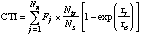
Figure 1 nicely illustrates this point.
(for a 3-
phase
CCD) and back to zero, as all traps are filled by some long preceding
deliberate or accidental charge packets to have been clocked out of the device.
Figure 1 nicely illustrates this point.
Fig. 1 From reference [14], effect of ionizing radiation damage on CTI, as
function of operating temperature.

This demonstrates the growth in CTI due to irradiation of a CCD with a
radioactive
 source. The density of Si-E centers increases, but the effect on CTI can be
minimized by operating at or below 190 K, where the trap emission time
becomes adequately long. The degradation in CTI below 160 K (even before
irradiation) is not seen in later CCDs from the same manufacturer. It probably
represents an artifact of the register design or processing of this particular
device. In practice, one can normally reduce the operating temperature to
~85 K before the CTI rises to ~
source. The density of Si-E centers increases, but the effect on CTI can be
minimized by operating at or below 190 K, where the trap emission time
becomes adequately long. The degradation in CTI below 160 K (even before
irradiation) is not seen in later CCDs from the same manufacturer. It probably
represents an artifact of the register design or processing of this particular
device. In practice, one can normally reduce the operating temperature to
~85 K before the CTI rises to ~
 at the onset of carrier freeze-out, the trapping of signal electrons by the
phosphorus donor ions [12]. This sets an effective lower limit to the useful
operating temperature of n-
channel
CCDs.
at the onset of carrier freeze-out, the trapping of signal electrons by the
phosphorus donor ions [12]. This sets an effective lower limit to the useful
operating temperature of n-
channel
CCDs.
For hadronic irradiation of CCDs, because of the much greater non-ionizing
energy loss or NIEL factor, the damage rates are greatly increased. In
addition, several donor-like defect levels have been identified. The Si-E
center (VP) still forms the predominant and deepest trap, though 15% of this
deep trap is believed due to the di-vacancy (VV) [16]. Shallower traps at
 are also observed [8, 16]. Protons are particularly damaging (due to the large
p-Si Coulomb scattering cross-section) and Fig. 2 shows the CTI resulting
from an irradiation with the very modest dose of
are also observed [8, 16]. Protons are particularly damaging (due to the large
p-Si Coulomb scattering cross-section) and Fig. 2 shows the CTI resulting
from an irradiation with the very modest dose of
 10 MeV proton/
 .
.
While these proton damage results are of great importance for their particular
application area (space-based X-ray cameras) they probably give a pessimistic
impression for the conditions relevant to particle detection systems, for two
main reasons. Firstly, these results refer to very low signal densities, so the
benefits of the long trap emission times at low temperature are not exploited
to the extent possible in a particle physics experiment. Secondly, the only
hadronic background likely to be significant at an
 collider are neutrons leaking through shielding. There is evidence that
neutrons may be much less harmful than would be inferred from these proton
data.
collider are neutrons leaking through shielding. There is evidence that
neutrons may be much less harmful than would be inferred from these proton
data.
Taking the standard NIEL factor, the data of Fig. 2 correspond to an
equivalent dose of 1 MeV neutrons of
 Yet there are measurements on n-channel CCDs (buried channel) [5, 6],
which demonstrate
Yet there are measurements on n-channel CCDs (buried channel) [5, 6],
which demonstrate
 for
for
 at room temperature. Most significantly [6], at a temperature of 84 K and
30 ms between bursts of charge injection, the CTI of
at room temperature. Most significantly [6], at a temperature of 84 K and
30 ms between bursts of charge injection, the CTI of
 is achieved for
 (1 MeV equivalent). The clocking conditions between these experiments are
quite different (protons in parallel register clocked very slowly, neutrons in
linear register clocked at 500 kHz) but this should not be critical. The low
temperature performance should be driven by the time between charge injections,
and 30 ms would be quite realistic for an HEP experiment. There is the
further difference that the neutron studies have all been made with large
signal packets, but as already discussed, this should become an issue only if
the packet size falls below ~1000
(1 MeV equivalent). The clocking conditions between these experiments are
quite different (protons in parallel register clocked very slowly, neutrons in
linear register clocked at 500 kHz) but this should not be critical. The low
temperature performance should be driven by the time between charge injections,
and 30 ms would be quite realistic for an HEP experiment. There is the
further difference that the neutron studies have all been made with large
signal packets, but as already discussed, this should become an issue only if
the packet size falls below ~1000
 ,
where the signal charge density falls significantly below the dopant level in
the n-channel.
,
where the signal charge density falls significantly below the dopant level in
the n-channel.
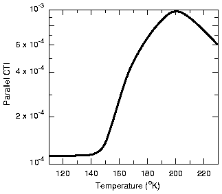
Fig. 2 From reference [16], effect of hadronic radiation damage on CTI,
as function of operating temperature. (10 MeV protons)
Conclusions
Due to their long readout time, CCDs are not applicable as vertex
detectors in continuous high flux environments such as LHC. They have a proven
record in fixed target experiments (where the incident beam can be interrupted
during the readout) and in the
 linear collider environment, where the interval between bunches (or between
bunch trains) allows time for readout. In both these environments, radiation
damage effects have so far been modest. In the fixed target environment, given
the small number of CCDs required, they can simply be exchanged at intervals of
6 months or so. For the
linear collider environment, where the interval between bunches (or between
bunch trains) allows time for readout. In both these environments, radiation
damage effects have so far been modest. In the fixed target environment, given
the small number of CCDs required, they can simply be exchanged at intervals of
6 months or so. For the
 collider, with reasonable care over beam conditions, the detector lifetime can
be many years.
collider, with reasonable care over beam conditions, the detector lifetime can
be many years.
For the future
 linear collider, the backgrounds may be substantially higher. The dumps for
secondary
linear collider, the backgrounds may be substantially higher. The dumps for
secondary
 pairs, for beamstrahlung and for the residual main beam, are all significant
sources of neutrons. At this stage, it is not clear if any of these could cause
problems for a CCD vertex detector. As we have seen, there is a possible
discrepancy between the radiation damage data with neutrons and with protons,
as regards charge transfer efficiency, so the actual performance limits for a
CCD detector are far from clear.
pairs, for beamstrahlung and for the residual main beam, are all significant
sources of neutrons. At this stage, it is not clear if any of these could cause
problems for a CCD vertex detector. As we have seen, there is a possible
discrepancy between the radiation damage data with neutrons and with protons,
as regards charge transfer efficiency, so the actual performance limits for a
CCD detector are far from clear.
What is long overdue is a comprehensive study of the radiation effects in one
CCD design, comparing electromagnetic, neutron and charged hadron irradiation,
with particular attention to the operating conditions (clocking, charge
injection interval and temperature), covering the region of interest for
particle detection. It should be noted that very high clocking rates for the
readout register (~50 MHz) are envisaged for this environment. This will
provide a significant suppression of CTI in this register due to the fact that
 will no longer be much larger than
 ,
so the above-mentioned fill factor can be far from unity. Equally important as
these systematic studies of radiation effects is a serious evaluation of
neutron background conditions likely to be encountered at the future
,
so the above-mentioned fill factor can be far from unity. Equally important as
these systematic studies of radiation effects is a serious evaluation of
neutron background conditions likely to be encountered at the future
 linear collider (the next likely application area for a large scale CCD vertex
detector). This work will reveal if there are any problems with the continued
use of currently available CCDs in our field. Should there be difficulties with
the anticipated neutron fluxes, there may be considerable room for improvements
in the CCD design. The most obvious step (analogous to the use of
hetero-structures in radiation hard GaAs electronics) would be to reduce the
storage volume for the charge packets. This is possible in both dimensions
orthogonal to the transfer direction, by the techniques of a narrow channel,
and a highly doped shallow channel. It should be remembered that for min-I
detection, a pixel well capacity of
linear collider (the next likely application area for a large scale CCD vertex
detector). This work will reveal if there are any problems with the continued
use of currently available CCDs in our field. Should there be difficulties with
the anticipated neutron fluxes, there may be considerable room for improvements
in the CCD design. The most obvious step (analogous to the use of
hetero-structures in radiation hard GaAs electronics) would be to reduce the
storage volume for the charge packets. This is possible in both dimensions
orthogonal to the transfer direction, by the techniques of a narrow channel,
and a highly doped shallow channel. It should be remembered that for min-I
detection, a pixel well capacity of
 would be entirely adequate; on current CCDs the signal charge floats around in
a vastly excessive storage volume. Another option would be to consider
p-channel devices, for which the Si-E center would be avoided. There is
some evidence [10] that such CCDs do have enhanced radiation hardness, though
this has not been studied with neutrons.
would be entirely adequate; on current CCDs the signal charge floats around in
a vastly excessive storage volume. Another option would be to consider
p-channel devices, for which the Si-E center would be avoided. There is
some evidence [10] that such CCDs do have enhanced radiation hardness, though
this has not been studied with neutrons.
In short, there is currently a need for background simulations and for
measurements with neutron irradiation of modern CCDs, to determine if the
future linear collider presents significant radiation damage problems for a
CCD-based vertex detector. Should there be such problems, the CCD designer has
a variety of tools at his disposal with which to improve the radiation hardness
of his designs. Many of these ideas will in any case be developed for non-HEP
applications in radiation environments, but the conditions specific to a
particle tracking detector do present opportunities that would not be
universally available.
References
[1] C J S Damerell et al, IEEE Trans Nucl Sci, 33 (1986)
51
[2] G D Agnew et al, Proceedings of the 26th International Conference on High
Energy Physics, Dallas 1992 (World Scientific, New York 1992), Vol 2,
1862
[3] K Abe et al, Design and Performance of the SLD Vertex Detector, a 307
Mpixel Tracking System, Nucl. Instr. & Methods (to be published)
[4] A M Mohsen and N F Tompsett, IEEE Trans. Electron Devices ED-21 (1974)
701
[5] G A Hartsell, Proc. Int. Conf. Appl., CCDs (1975) 375
[6] N S Saks, J M Killiany and W D Baker, Proc. NASA-JPL Conf. CCD Tech. &
Applications, Washington DC (1976)
[7] M G Collet, IEEE Trans. Electron. Devices ED-23 (1976) 224
[8] N S Saks, IEEE Trans. Nuclear Science NS-24 (1977) 2153
[9] J M Killiany, IEEE Trans Components, Hybrids & Manufacturing Technology
CHMT-1 (1978) 353
[10] N S Saks, J M Killiany, P R Reid and W D Baker, IEEE Trans. Nuclear
Science
NS-26 (1979) 5074
[11] J Killiany, Topics in Applied Physics 38 (1980) 147
[12] E K Banghart et al IEEE Trans. Electron Devices 38 (1991) 1162
[13] A Holland, A Holmes-Siedle, B Johlander and L Adams, IEEE Trans. Nuclear
Science 38 (1991) 1663
[14] M S Robbins, PhD Thesis, Brunel University (England) 1992
[15] I H Hopkins, G R Hopkinson and B Johlander, IEEE Trans. Nuclear Science
41 (1994) 1984
[16] S Watts, A Holmes-Siedle and A Holland
ESA Report BRUCRD-ESACCD-95-IR (1995)