INFRARED EMISSION: A NEW POSSIBLE APPROACH TO PARTICLE DETECTORS
G. Carugno*
INFN, Sezione di Padova, Via Marzolo 8, Padova, Italy
* e-mail address: carugno@pdinfn.it
Abstract
A brief review on the infrared concepts and photodetectors will be summarized. Emission of infrared photons has been observed in an ionization chamber filled with standard gases and some results are reported. Light produced by the electron drifting in the gaseous media has also been observed. Results are presented as a function of the electric drift field.
1. INTRODUCTION
Few data are available in the literature about the correlation between the ionization phenomena and the infrared (I.R.) signals (the typical range of the I.R. photon energy is between 0.01 and 1 eV).
The reported experimental data [1] only concerns the area near the I.R. region (£ 900 nm). This was possible using a GaAs photomultiplier (Q.E. = 20% up to 900 nm). Studying proportional scintillation in noble gases, some groups [2] stated a possibility of further emission in the wider I.R. region. In fact an incomplete energy balance in the photon emission process was seen.
Another unsolved question is related to the energy resolution in cryogenic noble liquid detectors, and the possibility of some energy output in the I.R. channel [3], according to a dimeric deexcitation. This is why we started our measurements hoping that some I.R. process occurs due to prompt or proportional scintillation. We also noticed that the drifting electron energy under the electric field (Eelectron = e * ![]() * l ª 0.2 eV), and the I.R. photon energy yield the same order of magnitudes.
* l ª 0.2 eV), and the I.R. photon energy yield the same order of magnitudes.
We speculate that due to the low energy quanta involved, the energy resolution can be improved with a high I.R. light yield scintillator
In the last few years, after the end of the cold war, good photodetectors have been made available to detect photons in the infrared region. The progress in I.R. technology has been largely used in astrophysical measurements.
For our purpose there are two kinds of useful I.R. sensors: photo-voltiac and photo-conductive. They can reach, under a controlled and cooled environment, a quantum efficiency of up to 80% at a 10 m m wavelength, with a possibility of detecting a few thousands of I.R. photons.
The I.R. materials, optics [4], and detectors [5] are available from many vendors. One of the limits affecting this field is the high cost of these devices compared to those devices which are sensitive in the visible wavelength region.
Due to the blackbody radiation representing a major drawback for I.R. particle detectors, the reader is reminded in Chapter 2 of some of the concepts on I.R. radiation and the present state-of-the-art in I.R. materials, detectors and handling methods. In Chapter 3 and 4, we present our measurements. In Chapter 5, we will consider the possible directions of future research in the field of high-energy detectors.
2. INFRARED PRIMER GUIDE
2.1. Infrared Radiation
The I.R. wavelength region ranges from 0.75 m m (1.65 eV) to a few 100m m (ª MeV). The I.R. region is usually subdivided in three regions: near (0.75¸ 3 m m), middle (3¸ 6 m m), and far (6¸ 15m m), respectively. Each region corresponds to different kinds of photodetectors.
Objects at a temperature higher than 0 ° K radiate due to the blackbody radiation. There are three main formulas governing the blackbody radiation:
1) Planck’s blackbody radiation law
Wl = c1 ![]() -5 [exp (c2 /
-5 [exp (c2 /![]() T) -1]-1 [Watt / cm2 m m]
T) -1]-1 [Watt / cm2 m m]
T = absolute temperature [° K]; ![]() = wavelenght [m m],
= wavelenght [m m],
c1 = 3. 74 * 104 [Watt m m4 / cm2 ] c2 = 1. 43 * 104 [m m ° K].
2) Stefan - Boltzmann law
W = s T 4 [W / cm 2 ] s = 5.66 * 10-12 [Watt/cm 2 ° K4 ].
3) Wien displacement law
![]() max * T = 2 8 9 7 [m m ° K].
max * T = 2 8 9 7 [m m ° K].
Figures 2.1 and 2.2 show the Planck radiation law expressed in terms of spectral radiant photon emittance.
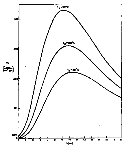
Figure 2.1. Planck’s law for spectral radiant emittance at three background temperatures TB.
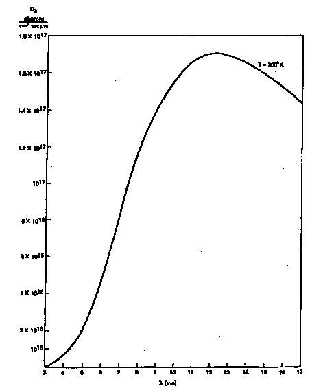
Figure 2.2. Planck’s law for spectral photon emittance at a background temperature of 300
° K.The objects are not usually ideal blackbody sources; i.e., the emissivity of the material must be taken into account (W’ = e W). Highly reflective metallic surfaces or I.R. transparent materials typically have a very low emissivity (see Figure 2.3 for details).
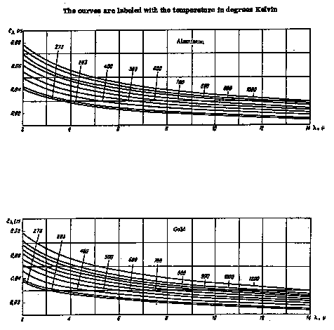
Figure 2.3. Spectral emissivity
e of aluminum and gold in the infrared region.A huge number of photons emitted from a blackbody source per cm2/sec makes it difficult to detect transient I.R. signals. Cooling down the entire system (detector + emitting material) helps. For example, the emission peak wavelength of 10 m m at 270° K shifts down to about 50 m m at 77° K, while the overall photon flux decreases from 1018 photons/cm2/s down to 1011 photons/cm2/s.
Another possibility to reduce the continuous blackbody emission is to select a particular I.R. line using very low bandwidth filters. This can decrease the background photon flux by many orders of magnitude.
2.2. Optical Materials
Another useful I.R. characteristic is the larger wavelength with respect to the visible one, which considerably decreases the scattering through the media.
The I.R. transmission through the atmosphere involves absorption in well-defined wavelength ranges due to H2O, O2 , and CO2 molecules, see Figure 2.4 and Ref. 6. Care must be taken in choosing the optical transmitting material and the presence of pollutants on the surfaces.
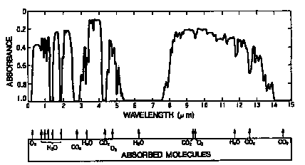
Figure 2.4. Atmospheric absorption above seawater.
The common materials used for I.R. optics such as lenses or windows are shown In Figure 2.5. The degree of transmission for these materials depends on the refractive index [6]. It can easily reach almost 100% with the help of antireflection coating as shown in Figure 2.6 for germanium window.
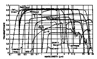
Figure 2.5. Transmittance of optical materials in the infrared region.
Figure 2.6. Transmittance of a germanium plate with and without antireflection coating.
Aluminum or gold-coated mirrors have a reflectivity of 99%. By means of I.R. emission lines, it is possible to use coated surfaces, e.g., the Febry-Perot cavity in order to have reflectivity as high as 99.99%.
2.3. I.R. Photodetectors
The most suitable detectors for our purpose are the quantum type [7]. The electrons, excited by the I.R. photons in the conduction band, give rise in some semiconductors a detectable current.
Because of the low photon energy, typically ~0.1 eV, it is necessary to cool down the detector to reduce the thermally excited currents in the semiconductor. Recently, Hamamatsu Co. marketed a cooled photomultiplier extending the photocathode quantum efficiency up to 1.7 m m. Most of the detectors are specially packaged to decrease the field of view angle (FOV) in order to reduce the background photons from the blackbody radiation and to optimize the level of the signal. Accurate measurements of low light level signals are made possible using a heterodyne detection method to suppress the blackbody background. This technique allows to detect signals as low as 10-20 W/Hz [8].
The glossary of I.R. detector technology takes into account the blackbody background because in these systems both the room temperature environment and the main phenomenon to be detected are normally involved. Such photodetectors are Background Limited Infrared Photo-detection "BLIP" limited.
The three main parameters characterizing the I.R. detectors are Responsivity (R), Noise Equivalent Power (NEP), and the normalized Detectivity (D*) [6]. The Responsivity (R) is the output current or voltage per watt. It is detector dependent when noise is not considered;
R = ![]() (A/W) P.V. or (V/W) P.C. ,
(A/W) P.V. or (V/W) P.C. ,
S = Signal output (A) or (V); P = Incident power/cm2 (W/cm2 ),
A = Detector area (cm2).
The Equivalent Power (NEP) sets the detection limit of the detector, and it is expressed in (W/Hz 1/2 ):
NEP = ![]() =
= ![]() ,
,
N = noise output (V) or (A),
D f = noise bandwidth (Hz).
The Detectivity (D*) allows the possibility to make a comparison between different detectors; it is normalized to 1 cm2 and 1Hz amplifier bandwidth:
D* = ![]() =
= ![]() ( cm Hz 1/2 /W = Jones).
( cm Hz 1/2 /W = Jones).
The D* values are quoted for a given measurement condition depending on the temperature of the radiant source, chopping frequency, and amplifier bandwidth. The D* limit, computed from theoretical considerations [6] only taking into account the I.R. blackbody background, for photo-voltaic (PV) and photoconductive (PC) detectors:
D*(PV) = ![]() x 1/2 /(2Q)1/2 (cm Hz 1/2 /W),
x 1/2 /(2Q)1/2 (cm Hz 1/2 /W),
D*(PC) = ![]() x 1/2 /Q1/2 (cm Hz 1/2 /W),
x 1/2 /Q1/2 (cm Hz 1/2 /W),
where l is wavelength, x is the quantum efficiency, h is the Planck constant, c is the speed of light and Q is the flux of background radiation.
As shown in Figure 2.7, the manufacturers quote the Detectivity of their products for the ‘’BLIP’’ conditions to 300 ° K radiant source, and FOV of 180° . Table 1 shows the typical Detectivity values for quantum type detectors [5]. The I.R. detectors currently used are BLIP limited. Therefore, the Detectivity can be increased by many orders of magnitude when cooling the external environment of the detector. For example, the Detectivity value of the InSb semiconductor at 5 m m with x = 70%, FOV = 180° , radiant source at 500° K, chopper frequency at 1200Hz, and 1Hz amplifier bandwidth is 1010 . If the radiant environment is cooled down to 77° K, its Detectivity increases to 1015.
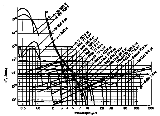
Figure 2.7. Detectivity for various infrared photodetectors (the BLIP curves are plotted for 300
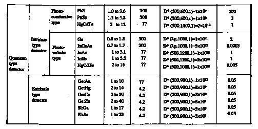
° K, 180° FOV.Table 1 - Quantum types Infrared Photodetectors and their characteristics.
I.R. detectors have sensitive surfaces of up to 1 cm2. It is possible to increase the surface by a factor of 20 or more with special lenses [7]. I.R. sensitive CCD detectors are also available on the market, with wavelengths of up to ~10 m m.
Photoconductive devices are useful for R&D purposes; however, they are slow devices (switch mode) requiring the light pulse time to be higher than the carriers lifetime, typically at 100 nsec.
We started our measurement with a MCT PC photodetector. Our MCT detector [9] has the following characteristics: working temperature = 77° K, FOV = 60° , detector area =
1 mm2 , Responsivity = 5000 V/W, NEP = pW/Hz1/2 , risetime = 0.5 m sec, D* (500, 1000, 1) = 4.1010 (cmHz 1/2 /W), QBLIP ª 1018 photons/cm2/s (300° K), and infrared window = ZnSe. The overall spectral response is shown in Figure 2.8. The maximum wavelength response is about 12 m m (5000 V/W).
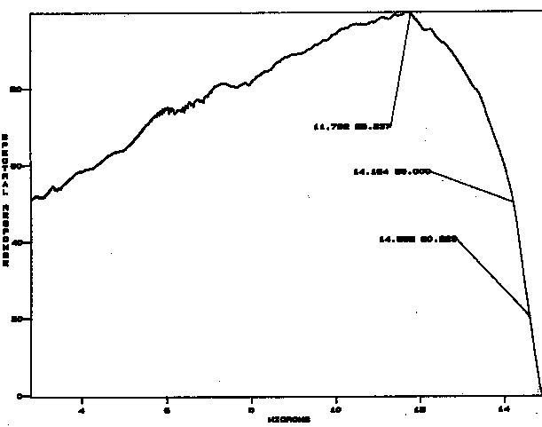
Figure 2.8. MCT P.C. photodetector response in the infrared sensitive region.
3. INFRARED SCINTILLATION IN THE GASEOUS MEDIA INDUCED BY IONIZING MEDIA
We started our investigation looking at standard gaseous systems used to fill an ionization chamber (I.C.). The experimental setup is shown in Figure 3.1.
Protons of 4 MeV from the Legnaro Van der Graaf facility (INFN Nat. Lab.) entered the I.C.. The continous proton beam was chopped with a rotating wheel, generating a time-window of about 100 m s every millisec, and 105¸ 106 protons were contained in each window. The protons entered the I.C. through two 10 m m Mylar windows, and were stopped and measured in the Faraday cup. The approximate energy release per proton in the I.C. at N.P.T was of the order of a few hundred keV. The I.R. sensor (see Fig. 3.1.) was placed perpendicularly relative to the beam direction. The solid angle covered by the sensor was
10-3. The I.C. was made from two metallic plates, 2 cm apart and a diameter of 2 cm. The one closest to the sensor was made of wires with 1 mm spacing. The cell was rated up to 6 bar. The optical coupling between the I.R. sensor and the I.C. was realized via a ZnSe window. The transmitting wavelength was higher than 750 nm. The ZnSe material is not wave-shifting, and stops the known U.V. scintillation emission [9] from the noble gases.
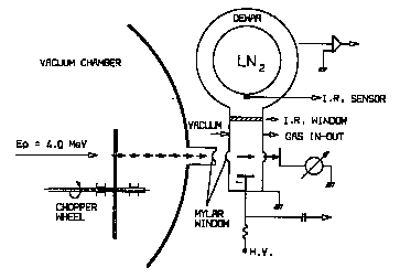
Figure 3.1 - Schematic view of the experimental apparatus (not in scale).
The following gases were tested: He, Ar, Kr, Xe, CO2 , CH4 , and N2 . Some of them are known to be transparent to I.R. radiation (noble gases and N2). The scintillation was clearly seen only with the noble gases. Helium gave a weaker signal compared to the others. The I.R. emission phenomenon seems to be independent from pressure conditions. The power detected on the I.R. sensor was at a level of a few m W. Our study focused on Argon gas in the pressure ranges from 0.2 to 5.5 bar. A typical I.R. signal from the MCT detector is shown in Figure 3.2.
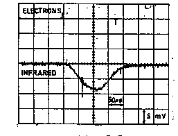
Figure 3.2. Infrared scintillation signal for Argon gas (T = 290
° K, P = 1.7 bar). No electron current signal ispresent (
D V = 0 in the I.C. electrodes). In order to understand the emission spectra, we used materials with different transmission characteristics between the I.R. sensor and the I.C. window. The result is the emission wavelength centered between 1 and 2 m m. These measurements are very preliminary and we are planning to make a systematic study with a spectrophotometer to measure more precisely the emitting wavelength. This emission line is probably related to dimeric deexcitation of the Ar2 [10] molecule formed by ionization. If this is the case, the Xenon should emit around 2 m m [11]. We have compelling reasons to believe that scintillation is also present in the liquid phase. We are preparing a cryogenic test cell to be irradiated with an electron beam to look for the I.R. radiation. As stated before, the cryogenic environment reduces dramatically the blackbody background. This gives rise to the possibility of using simple Ge or InGaAs photodiodes in case of liquid Argon.![]() We intend to look at other materials, liquid and solid, emitting in the I.R. wavelength region.
We intend to look at other materials, liquid and solid, emitting in the I.R. wavelength region.
4. INFRARED EMISSION BY DRIFTING ELECTRONS IN GAS
We noted that the I.R. signal was increased in all noble gases after switching on the electric field in the I.C. In Nitrogen, the I.R. signal, which was not seen in the "prompt mode," appeared when the drift-field was applied. The increase in the I.R. signal is clearly visible in Figure 4.1 for Argon gas. The dependence of the I.R. amplitude on the voltage applied to the I.C. for Argon at 5 bar is shown in Figure 4.2. In the same figure, we show the collected charge as a function of the applied voltage. It was possible to remove the prompt scintillation light by placing a filter between the sensor and the window. The light emitted during the electron drifting was above 2 m m wavelength.
The mechanism involved in ifrared emission is different from the prompt scintillation. The emission light created by the drifting electrons may be related to some excitation of the gas. The onset of such phenomena can be observed at very low electric fields (see Figure 4.2). Up to now, we have not succeed in understanding whether this emission is continuous or a line spectrum.
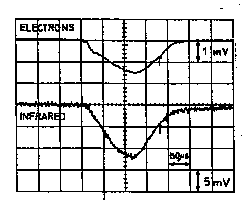
Figure 4.1. Electron current signal (
D V = + 1500) and infrared signals (prompt + electron drift superimposed).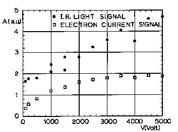
Figure 4.2. Current and I.R. light signal (arbitrary units) vs voltage applied to ionization chamber.
As seen in Figure 4.3, the drifting electrons seem to have excited the Nitrogen molecules in vibrational states, whose lifetime is of the order of a millisecond. This would support the idea of line emission.
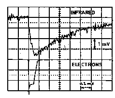
Figure 4.3. Electron current and I.R. light signal in Nitrogen.
The drifting emission in the noble gases seems to be quite efficient and doesn’t show any decrease at higher pressure.
The measurements we have obtained are considered preliminary. The investigation can be extended using materials where electrons show high mobility.
5. SUMMARY AND PERSPECTIVES
ACKNOWLEDGEMENTS
The author is specially indebted to E. Conti for his continuos help and advise during the beam time run at the Legnaro National Lab. I would like to thank A. Meneguzzo, F. Borghesani, G. Bressi, P. Calvani, and D. Zanello for stimulating discussions on the subject.
REFERENCES
[1] P. Lindblom, O. Solin, NIM A268 (1988) 204.
[2] R. D. Andersen et al., NIM 140 (1977) 371.
A. Policarpo et al., NIM 102 (1972) 337.
[3] Masuda et al., NIM 160 (1979) 239.
[4] II - VI Incorporated, PA, USA.
[5] E.G.G. Judson Optoelectronics; Hamamatsu Ind.; Fermionics IR Ind.
[6] Hamamatsu Infrared Technical Information.
[7] E. Dereniak, D. Crowe; Optical Radiation Detectors; Wiley & Sons (1984).
[8] Optics-Handbook, VOL. I, (15).
[9] E.G.G. Judson Optoelectronics, I.R. Detector.
[10] D. C. Lorents Physica, 82 C (1976) 19.
[11] H. A. Köhler et al., Phy. Rev. A 9, 2 (1974) 768.