R.Bouclier, M.Capeáns, W.Dominik, M.Hoch, J-C.Labbé, G.Million, L.Ropelewski, F.Sauli and A.Sharmaa
CERN, CH-1211 Genève, Switzerland
a VUB-ULB Brussels, Belgium
Multiple GEM grids in the same gas volume allow to obtain large amplification factors in a succession of steps, leading to the realization of an effective gas-filled photomultiplier.
I. INTRODUCTION
Methods for obtaining large, stable proportional gains in gaseous detectors are a continuing subject of investigation in the detector's community. Several years ago, Charpak and Sauli [2] introduced the Multi-Step Chamber (MSC) as a way to overcome some limitations of gain in Parallel Plate and Multi-Wire Proportional Chambers (MWPC); two parallel grid electrodes, mounted in the drift region of a conventional gas detector and operated as parallel plate multipliers, allow to pre-amplify drifting electrons and transfer them into the main detection element. Operated with a photo-sensitive gas mixture, the MSC allows to reach gains large enough for single photon detection in Ring Imaging Cherenkov (RICH) detectors [3].
More recently, Charpak and Giomataris have developed MICROMEGAS, a high gain gas detector using as multiplying element a narrow gap parallel plate avalanche chamber [4]. With gaps in the range 50 to 100 um, realized by stretching a thin metal micro-mesh electrode parallel to a read-out plane, the authors have demonstrated very high gain and rate capabilities, understood to result from the special properties of electron avalanches in very high electric fields.
The major practical inconvenience of both described detectors lies in the necessity of stretching and maintaining parallel meshes with very good accuracy; the presence of strong electrostatic attraction forces adds to the problem, particularly for large sizes. This requires heavy support frames, and in the case of MICROMEGAS, the introduction in the gap of closely spaced insulating lines or pins with the ensuing complication of assembly and loss of efficiency.
An interesting device recently developed, the CAT (Compteur A Trou [5]), consists of a matrix of holes drilled through a cathode foil; with the insertion of an insulating sheet between cathode and buried anodes, it allows to guarantee a good gap uniformity and to obtain high gains.
In the present paper, we describe a novel concept that seems to hold both the simplicity of the MSC scheme, and the high field advantages of MICROMEGAS and CAT, however mechanically much simpler to implement and more versatile: the Gas Electron Multiplier (GEM).
II. PRINCIPLE OF OPERATION
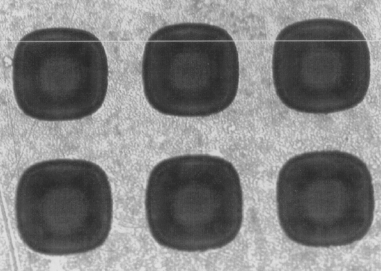
The basic element of the GEM detector is a thin, self-supporting three-layer mesh realized by the conventional photo-lithographic methods used to produce multi-layer printed circuits. A thin insulating polymer foil metallized on each side is passivated with photo-resist and exposed to light through a mask; after curing, the metal is patterned on both sides by wet etching and serves as self-alignment mask for the etching of the insulator in the open channels. We have obtained medium size meshes (5 by 5 cm2) with 25 um thick polymer sandwiched between 18 um thick copper electrodes; the etching pattern has rows of 70 um wide holes spaced 100 um (Fig. 1); the fabrication technology, developed by the CERN Surface Treatment Service[1], can be extended to larger areas.
Fig. 1: Micro-photography of the three-layer (metal-insulator-metal) GEM grid. The distance betwen holes is 100 um.
Because of the etching process, holes are conical in shape from both entry sides, probably improving the dielectric rigidity (see Fig. 2). Upon application of a suitable difference of potential, the electric field in a channel of the GEM grid develops as shown in Fig. 2; for this calculation, the mesh has been inserted between two equidistant electrodes at symmetric potentials. From the data reported by the authors of Ref. 4, we expect to obtain multiplication in the high field in the center of the channel at a difference of potential around two hundred volts; for this value, the corresponding field strength along the central line is shown in Fig. 3: at the maximum, it reaches 40 kV cm-1. Electrons produced by ionization in the upper gas volume drift into the channels, multiply in avalanche in the high field region and leave towards the electrodes in lower volume. Most of the ions generated in the avalanche recede along the central field lines, limiting the perturbing effects of the insulator charging up.
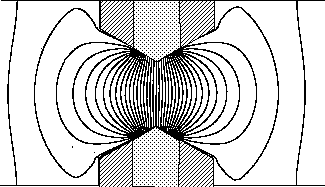
Fig. 2: Equipotentials lines in the GEM multiplying channel (VGEM =200V).
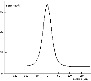
Fig. 3: Electric field along the central field line in the multiplying channel.
Thanks to the focusing effect of the field, one expects full efficiency for transfer of charge, and the dense channel spacing reduces image distortions. For the device to properly function, a good and regular insulation between the grid electrodes is required, with no sharp edges, metallic fragments or conducting deposits in the channel; this has been obtained by careful optimization of the etching and cleaning procedures. The first GEM mesh manufactured on our design had around a quarter million channels covering a square grid 50x50 mm2, and was used for the measurements described in what follows. The test assembly is schematically shown in Fig. 4: a standard, small size MWPC is modified replacing one cathode with a thin printed circuit board holding the GEM mesh in the center; the mesh is pasted to the board, taking great care to avoid problems at the outer edge of the print (the metal on one side of the grid was removed for a few mm along the edges). Above the GEM electrode, a second cathode (the drift electrode) defines the sensitive volume of the detector.
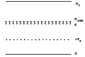
Fig. 4: Test assembly with the GEM multiplier mounted within a standard MWPC (drawing not to scale).
For convenience, the MWPC is operated with the anode wires at positive potentials, the signals being picking up through HV decoupling capacitors; this choice allows to maintain the lower electrode of GEM at ground potential, and easily increase the multiplying voltage. For ionization produced in the MWPC gaps, a regular process of collection and amplification takes place; electrons released in the upper drift region, on the contrary, can drift into and through the GEM channels and multiply, depending on potentials. Using a collimated X-ray source, one can easily disentangle the operation in the two regions. For most of this study, we have used a 5.9 keV 55Fe X-ray source; to measure the rate capability, the detector has been exposed to a collimated 8 keV beam from a generator.
III. EXPERIMENTAL RESULTS
A. Charge transfer and pre-amplification
In order to avoid having to reach excessive potentials across the GEM mesh, we have found convenient to operate the detector at low quencher levels; a good choice is a mixture of Argon and Dimethyl-ether (DME) in the proportion 90-10, used for all measurements described here. The detector operates however well in other mixtures, including some with the level of quencher below the flammability limit (3.5% for DME). The MWPC is powered at a voltage providing a moderate gain (~104), keeping VGEM grounded; the standard 55Fe spectrum is recorded. With the upper drift electrode at fixed potential (typically -1 kV), the negative potential on GEM is progressively increased. At -VGEM~ 50 V, a signal begins to appear, corresponding to charge transferred from the drift region; at ~ 140 V the transferred charge equals the direct one (100% transparency). Increasing -VGEM further, the pre-amplified charge exceeds the direct component. Fig. 5 shows a typical pulse height spectrum, recorded at a pre-amplification factor around 6:
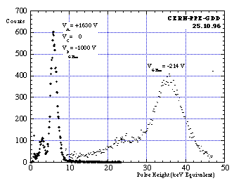
Fig. 5: 55Fe pulse height spectrum recorded in the MWPC without (left) and with pre-amplification.
The energy resolution of the detector is not affected by the pre-amplification process; from Fig. 5 one can infer a resolution of around 11% r.m.s. for the pre-amplified charge, as compared to 12% r.m.s. for the direct signal (the apparent improvement is probably due to some non-linearity of the response)
Fig. 6 shows the measured pre-amplification factor, defined as the ratio of the most probable pulse height between transferred and direct spectra for the 5.9 keV line, as a function of the GEM voltage. In this particular mesh, the first to be realized, discharges appear at around -230 V; they are however without any consequence to the detector. From previous observations [6], we expect that use of a thicker insulator (50 to 100 um instead of 25) could lead to higher effective gains.
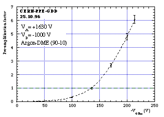
Fig. 6: Pre-amplification factor as a function of the difference of potential on the GEM grid.
The strength of the field in the drift region does not affect, in a wide range, the collection and transfer characteristics and the pre-amplification factor (although it affect other drift properties). We have seen no difference in transferred charge, at a pre-amplification factor around 6, varying the drift voltage from -500 to -2000 V. This can be exploited to tune drift velocity, diffusion and Lorentz angles according to experimental needs.
B. Uniformity of response
The uniformity of response of the detector has been measured by displacing the collimated source across the active area (50x50 mm2); the gain is remarkably uniform (Fig. 7), with a maximum variation of +/-4% (which includes the possible variations in the MWPC). Because of poor collimation of the source, the signal is detected on a slightly wider region than the opening of the grid.
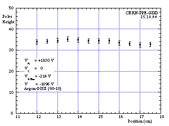
Fig. 7: Gain uniformity measured across the GEM grid.
C. Rate capability
To investigate possible gain reductions induced by charges deposited on the insulator surfaces within the channels, we have exposed the GEM detector to increasing rates of 8 keV X-rays from a generator. The irradiated area covered about 3 mm2. It should be noted that the MWPC itself (with 2 mm wire spacing) is expected to suffer space charge gain drops at rates exceeding ~ 104 mm-2s-1. In order to be in similar conditions, the measurements were realized at constant total gain adjusting the MWPC anode potential. The preliminary results, Fig. 8, show no difference in behavior implying the absence of charging up processes in the GEM mesh.
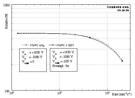
Fig. 8: Gain as a function of rate measured at equal gain for the MWPC and for the GEM+MWPC chamber.
Coupled to a high-rate detector, such as the MSGC, the rate capability of GEM may be limited by charging-up of the insulator in the open channels. If such is the case, it can be envisaged either to use a moderate conductivity material for the layer (in the range 1010 to 1013 [[Omega]].cm), or to coat the mesh by vacuum deposition or Chemical Vapor Deposition (CVD) with a thin controlled resistivity layer in the range 1014 to 1016 [[Omega]]/q, using technologies developed for MSGCs [7].
IV. APPLICATIONS
A variety of uses can be envisaged for the GEM mesh: self-supporting, the element can be easily incorporated in other structures. The added pre-amplification factor, even moderate, can ease the operation of any gain-critical detector.
In Micro-Strip Gas Chambers (MSGC) a serious problem of discharges has been met recently [8,9]. When operated close to their maximum gain limit in order to efficiently detect minimum ionizing particles, MSGCs can be irreversibly damaged by a discharge initiated by heavily ionizing tracks (recoils produced by neutrons, nuclear fragments); the effect is enhanced in presence of a high flux of radiation, and its probability depends strongly on the operating voltage [10]. The use of a GEM grid above the MSGC, with even a moderate pre-amplification, would allow to operate the MSGC well below the critical potential for discharges. The moderate increase in the spatial extension of the detected charge, with its de-clustering effect, should also improve the localization accuracy; the added delay, corresponding to the drift time of electrons from GEM to the MSGC plate, could be exploited for the first level triggering.
A second application of the pre-amplification principle, already mentioned, could be in fast RICH detectors. Aside for allowing larger gain and therefore easing single photo-electron detection, the structure can be designed to exert a high electric field on the solid photo-cathode side of the detector, thus substantially improving its quantum efficiency [11]. Fig. 9 shows schematically an "improved" fast RICH detector with pad read-out on the MWPC cathode. The presence of the GEM mesh between the main amplification element and the photo-cathode should also reduce the possibility and the dangerous effects of photon feedback.
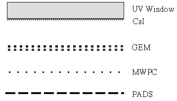
Fig. 9: Fast RICH detector with pre-amplification.
The GEM grid can easily be used as controlled gate to prevent ions feedback, or to select event similarly to the scheme used in pulse-gated Time Projection Chambers; the small value of the gating voltage would greatly reduce pick-up problems.
All described results have been obtained with a rather thin mesh (25 um) resulting in a short multiplication path for electrons and therefore moderate gains. According to the authors of Refs. 4 and 5, in a parallel plate geometry the best results in terms of gain have been obtained for gaps close to 100 um; if thicker GEM meshes provide similar results, one can envisage to replicate the MICROMEGAS and CAT high gain performances performances by simply laying a mesh over the stripped readout electrode; being cheap and self-supporting, this geometry should have definite advantages over the quoted designs.
Perhaps the most original use of GEM would be in a multi-stage gas electron multiplier, as shown in Fig. 10. Several composite grids, mounted within the same gas volume, and powered by a suitable resistor chain should allow to reach large gains, somewhat in analogy to multi-grid vacuum tubes, but substantially simpler and cheaper to manufacture for large areas; readout could be obtained with a terminal MWPC, MSGC or directly on a matrix of pads. The multiplier should operate in strong magnetic fields, with only some image distortions (Lorenz angle). For large gains, ions feedback and attachment to the insulator may become a problem, and should be studied.
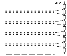
Fig. 10: A multi-grid GEM multiplier; read-out can be realized directly on strips or pads, or using a MWPC, MSGC or PPC.
As a final suggestion, one can think of developing non-planar GEM structures for special applications, cylindrical for tracking detectors around colliders and spherical for resolving the well know parallax error aberration in thick layer X-ray detectors such as those used for crystal diffraction studies
V. FURTHER DEVELOPMENTS
Much of the described applications and developments depend on the elaboration of a suitable, reliable technique to produce the GEM grids at low cost. Intrinsically simple and making use of well established printed circuit technologies, manufacturing of the multi-layer grids is nevertheless a delicate enterprise in view of the requirements (very good insulation between the two metals). Careful cleaning, not introducing any sort of conducting debris or stains, should be used, followed by proper conditioning; we have found that baking in vacuum at moderate temperature (~ 100 deg.C) improves the quality of the insulation. With CERN installations, good quality prints with 20 cm on the side can be manufactured today; larger sizes would require recourse to outside industry. Alternative methods for realizing the GEM structure are being investigated; a promising approach makes use of existing polymer high-precision meshes used as filters in the chemical industry and vacuum-coated on both sides with a thin layer of metal [2].
The influence of the insulator thickness on the maximum gain has to be investigated, as well as the possible charging up effects; if relevant, these effects could be controlled by the use of a moderate resistivity insulator, or with a thin resistive coating applied by non-directional deposition technologies such as Chemical Vapor Deposition in analogy of what is done to solve similar problems in MSGCs. Other industrial processes, such as those used to produce the low cost, large size micro-meshed used in the electronics industry should be investigated.
VI. CONCLUSIONS AND SUMMARY
We have described a novel concept in gas amplification structures, a thin insulating mesh separating to two metal grids with a dense matrix of holes or channels, typically 50 um in diameter. Inserted in the path of drifting electrons, the Gas Electron Multiplier allows to transfer the charge with an effective amplification; pre-amplification factors close to ten have been obtained with GEM grid implemented on a 25 um thick insulator, but higher values can be expected with thicker layers (50 to 100 um). The GEM grid is relatively easy to manufacture using standard multi-layer printed circuit technology, and large sizes can be envisaged. Inserted as pre-amplification element in various types of gas detectors, the GEM amplifier should allow to overcome some limitations intrinsic in the use of gaseous devices at high gains.
All proprietary and other rights related to the information contained in this article are vested in CERN and its use by third parties is subject to prior written approval by CERN.
VII. REFERENCES
[1] F. Sauli,The Gas Electron Multiplier, submitted as Letter to Nucl. Instr. and Methods (1 Nov. 1996).
[2] G. Charpak and F. Sauli, Physics Letters 78B (1978) 523.
[3] M. Adams et al, Nucl. Instrum. Methods 217 (1983) 237.
[4] Y. Giomataris, Ph. Rebougeard, J.P. Robert and G. Charpak, Nucl. Instr. Meth. A376(1996)29.
[5] F.Bartol, M. Bordessoule, G. Chaplier, M. Lemonnier and S. Megtert, J. Phys.III 6(1996)337.
[6] R. Bouclier, M. Capeáns, G. Million, L. Ropelewski, F. Sauli, T. Temmel, R.A. Cooke, S. Donnel, S. Sastri and N. Sonderer, Nucl. Instrum. Methods A369 (1996) 328.
[7] R. Bouclier, M. Capeáns, C. Garabatos, G. Manzin, G. Million, L. Ropelewski, F. Sauli, T. Temmel, L. Shekhtman, V. Nagaslaev, Yu. Pestov and A. Kuleshov, Nucl. Instr. Meth. A365(1995)65.
[8] V. Peskov, B.D. Ramsey and P. Fonte, Int. Conf. on Position Sensitive Detectors (Manchester, 9-13 Sept. 1996).
[9] R. Bouclier, M. Capeáns, G. Manzin, L. Ropelewski, F. Sauli, A. Sharma, L. Shekhtman, CERN CMS TN/96-018.
[10] A. Breskin, Nucl. Instrum. Methods A371 (1996) 116.