 by the onset of breakdown. The microdot structures1,2, however,
possesses all the above qualities and are in addition able to sustain gains of
the order of
by the onset of breakdown. The microdot structures1,2, however,
possesses all the above qualities and are in addition able to sustain gains of
the order of
 .
.
THE MICRODOT GAS AVALANCHE DETECTOR
Department of Physics, University of Liverpool, P.O.Box 147
Liverpool L69 3BX, UK
ABSTRACT
The microdot gas avalanche detector is introduced and experimental measurements from the laboratory are described. Two separate batches of detector have been produced and results are presented showing the detectors gain dependence on cathode and drift voltage and the performance of such detectors to high intensity x-ray fluxes. The energy resolution at high rate and gain is also shown along with preliminary ageing measurements. Results obtained from single photo electron extraction by a UV source from the aluminium support of the drift cathode are presented at avalanche gains of up to 30000.
1 Introduction
Experiments at future high intensity colliding beam machines and at high
intensity synchrotron radiation facilities require a detector which has an
intrinsic high rate capability, good imaging or spatial resolution and
excellent stability in a high radiation environment. Microstrip gas avalanche
(MSGC) and microgap (MGAP) detectors with 200 micron pitch readout possess some
of these properties, but are limited to avalanche gains of <
by the onset of breakdown. The microdot structures1,2, however,
possesses all the above qualities and are in addition able to sustain gains of
the order of
.
2 Detector Manufacture
Microdot (MDOT) detectors of various geometries have been constructed on 4 in. diameter silicon wafers using a standard MOS processing line3. Figure 1 shows a schematic of one cell from above and in cross section through the substrate. The structure has been implemented with an underlying back plane bus enabling the anode
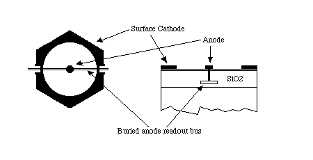
Figure 1: Schematic of microdot cell from above and in cross section
dots to be readout in strings which have been produced with both 100 and 200 micron readout pitch. The anode dots are typically 12 to 20 microns in diameter and the cathodes are between 20 and 40 microns wide. The anode cathode gap is of the order of 75 microns for a 200 micron pitch and 35 microns for a 100 micron pitch structure.
The processing steps used in the manufacture of the microdot structures are:
1. oxide deposit to 2.5
 depth
depth
2. metal 1 deposition and etch, 0.6 to 1
 thick
thick
3. second oxide deposition to 2.8
 depth
depth
4. ion implantation
5. oxide via etch
6. metal 2 deposition and etch, 1.5
 thick
thick
The surface of the insulating substrate is doped to a higher conductivity than the bulk to reduce charge up effects and the currents flowing in this layer control the field gradients across the substrate.
3 Detector Geometry
Two separate batches of MDOT detectors have been produced and the main differences between the two will be outlined below. During the production of the first batch of MDOTs, further electric field simulation4 showed that the anode readout bus was significantly distorting the electric field in the gas directly above the surface of the bus. The effect of this distortion was to create a potential well for electrons, created in the avalanche, into which they can fall and be focused onto the bus lines rather than the anode dots. To compensate for the effect a "floating potential" ring was added between anode and cathode which serves to restore symmetry to the electric field ensuring that the electrons focus onto the anode dots. This ring was thus incorporated into half of the first batch of the MDOTs and a schematic of the structure is shown in figure 2a.
During the testing of the first batch of detectors, it was found by optical inspection that the structures were suffering from "punch-through" breakdown. This manifests itself as a short circuit occurring at the cross over point between the anode bus line and the cathode, and was found to be developing at sites on the metal 1 layer where "hillocks" had formed. These are regions on the aluminium metal 1 layer where a movement of grain boundaries has occurred causing a raise in profile at the point.
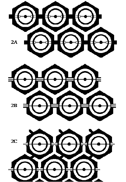
Figure 2: Schematic of the described microdot structures
This is a common occurrence in the semi-conductor industry and is due to the
high temperatures used during the deposition of the oxide layer. Thus for the
second batch of MDOTs that were produced the intermetal oxide layer was
increased in thickness from 1.8
 to 2.8
 .
The mask design was also improved to reduce the metalised area on the cathode
which covers the anode bus line. This serves to reduce capacity and improves
the reliability from punch-through breakdown between the metal 1 anode bus and
the metal 2 cathode, figure 2b. In addition to the above changes 2D structures
have also been produced, where the anodes are connected in strings along the
bus lines and the cathodes are connected in strings in an orthogonal direction
on the metal 2 layer, figure 2c.
.
The mask design was also improved to reduce the metalised area on the cathode
which covers the anode bus line. This serves to reduce capacity and improves
the reliability from punch-through breakdown between the metal 1 anode bus and
the metal 2 cathode, figure 2b. In addition to the above changes 2D structures
have also been produced, where the anodes are connected in strings along the
bus lines and the cathodes are connected in strings in an orthogonal direction
on the metal 2 layer, figure 2c.
4 Results
The absolute gain of the detector was determined in two ways. 1) calibration of the electronics chain by the injection of a pulse of known amplitude to the input capacitor of an Ortec 142AH preamplifier and 2) by monitoring the chamber current, performed using a Keithley 237 source measure unit (SMU) and the x-ray rate. The two methods agree to 10-15% which is consistent with the systematic errors. The presented results are obtained from the signal of 14 anode strings, each of length 6cm, for the 200 micron pitch structures and 28 strings for the 100 micron pitch structures, which are connected together and input to the preamplifier. No passivation was applied to the electrode ends.
4.1 Gain Measurements
The gas gain dependence of the MDOT structures on cathode voltage has
been investigated. Figure 3 shows this dependence for a 200
 pitch structure with floating rings from the first batch, in various Ar:DME gas
mixtures. The results were obtained using an Fe55 x-ray source at
low rate (~10cts/mm2/sec). The upper limit in each case was defined
by a current trip on the SMU of 20nA. This limit was determined from experience
with MSGCs and marks the onset of microdischarges or punch-through breakdown.
The upper limit of 12000 in the case of a 50:50 Ar:DME mixture is typically a
factor of 1.4 higher than that obtained with an MSGC on an electronic
conducting substrate5 and is obtained at a lower value of drift
voltage and a much reduced value of cathode voltage.The gain for these batch 1
detectors was
pitch structure with floating rings from the first batch, in various Ar:DME gas
mixtures. The results were obtained using an Fe55 x-ray source at
low rate (~10cts/mm2/sec). The upper limit in each case was defined
by a current trip on the SMU of 20nA. This limit was determined from experience
with MSGCs and marks the onset of microdischarges or punch-through breakdown.
The upper limit of 12000 in the case of a 50:50 Ar:DME mixture is typically a
factor of 1.4 higher than that obtained with an MSGC on an electronic
conducting substrate5 and is obtained at a lower value of drift
voltage and a much reduced value of cathode voltage.The gain for these batch 1
detectors was
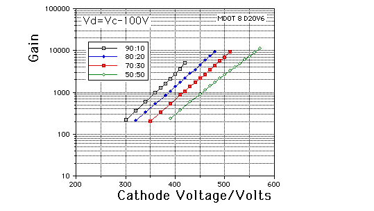 Figure 3: Gain curves for a 200 micron batch 1 structure with floating
rings
Figure 3: Gain curves for a 200 micron batch 1 structure with floating
rings
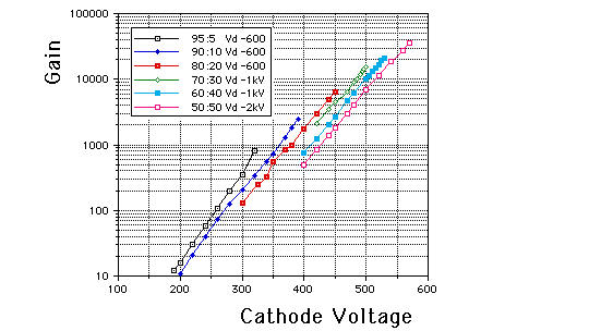 Figure 4: Gain curves for a 100 micron batch 2 structure
limited by punch through breakdown which was confirmed by optical inspection of the detector, manifesting itself as damage to the electrode structure. Figure 4 shows
the gain curves obtained with a 100
 pitch structure from the second batch of MDOTs. Gains of up to 40000 have been
measured and this coupled to the detectors low noise levels allows these
devices to be used to detect single photo electrons (see below). Results are
not presented for the batch 2 200
pitch structure from the second batch of MDOTs. Gains of up to 40000 have been
measured and this coupled to the detectors low noise levels allows these
devices to be used to detect single photo electrons (see below). Results are
not presented for the batch 2 200
 pitch structures but gains in excess of 50000 have been measured. Their
behaviour is not stable due to surface charging caused by a lack of surface
current in the implanted layer. This could be compensated for by reducing the
anode cathode gap or by modification of the conducting layer to decrease its
resitivity.
pitch structures but gains in excess of 50000 have been measured. Their
behaviour is not stable due to surface charging caused by a lack of surface
current in the implanted layer. This could be compensated for by reducing the
anode cathode gap or by modification of the conducting layer to decrease its
resitivity.
In the case of the second batch of MDOTs the ratio of gain measured on anodes
to the cathodes has been investigated and figure 5 shows this ratio for various
applied drift voltages and for various shaping times on an Ortec 571 post
amplifier. The applied cathode voltage in this case was -400V for the three
different values of drift voltage. The graph shows that for an applied drift
voltage of -1kV, corresponding to a drift field of
 ,
and at all values of shaping time that 85% of the anode signal is induced on
the cathodes. Simulation of the dependence of charge ratio on applied drift
field and integration time has been found to agree well with the experimental
results. The change in ratio at integration times below
,
and at all values of shaping time that 85% of the anode signal is induced on
the cathodes. Simulation of the dependence of charge ratio on applied drift
field and integration time has been found to agree well with the experimental
results. The change in ratio at integration times below
 is caused by the slow rise time of the preamplifier due to capacitive loading
caused by bussing a large number of the cathode strings into the preamplifier.
When this effect is removed the ratio is predicted to stay constant from
is caused by the slow rise time of the preamplifier due to capacitive loading
caused by bussing a large number of the cathode strings into the preamplifier.
When this effect is removed the ratio is predicted to stay constant from
 to below 500nS.
4.2 Energy and Spatial Resolution
The energy resolution of the MDOTs is determined using an 8keV x-ray
crystallography set, and figure 6 shows the resulting spectrum obtained at high
rate and high gain for a 200
 pitch batch 1 structure . A FWHM of 19% was obtained which compares well to
the 18% achieved with these structures at lower rates. Figure 7 shows an 8keV
spectrum taken with a 200
pitch batch 1 structure . A FWHM of 19% was obtained which compares well to
the 18% achieved with these structures at lower rates. Figure 7 shows an 8keV
spectrum taken with a 200
 pitch structure from batch 2 at a gain of ~1000 and gives a FWHM of 14% which
is limited by avalanche fluctuations.
pitch structure from batch 2 at a gain of ~1000 and gives a FWHM of 14% which
is limited by avalanche fluctuations.
The spatial resolution of the MDOT structures for minimum ionising particles
has been simulated using the MSGCSIM code6, which gives
 x=
x= y=16
to 18
y=16
to 18
 in the case of a 100
 pitch MDOT and
 x=
x= y=32
to 35
y=32
to 35
 for the case of a 200
 pitch structure. In both cases the simulation gives
 =6%
for the energy resolution for 6keV x-rays.
=6%
for the energy resolution for 6keV x-rays.
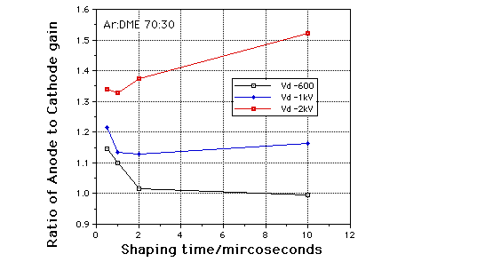 Figure 5: Ratio of anode to cathode gain for a 100 micron pitch batch 2
structure
Figure 5: Ratio of anode to cathode gain for a 100 micron pitch batch 2
structure
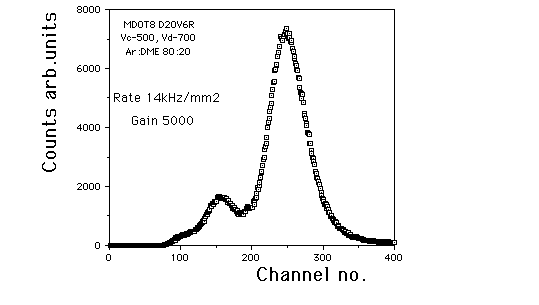 Figure 6: 8keV spectrum taken at high rate and high gain
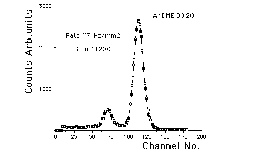 Figure 7: 8keV spectrum taken with batch 2 200 micron structure
4.3 Photo electron Spectra
The fact that the MDOT structures allow gains in excess of 10k renders
them able to detect single photo electrons and this has been investigated using
a 100
 pitch MDOT. For the following results the MDOT was operated between -510 and
-560V with a drift voltage of -1300V. A UV lamp source was incident at an angle
to the detector plane in order to extract photo electrons from the edge of the
aluminium frame supporting the drift cathode. This non ideal geometry was
forced due to the lack of a photo sensitive drift cathode. Despite this
problem, it was possible to measure about 30 pulses/second from electrons which
diffused into the first row of microdots in the fringe field of the detector.
The spectra obtained are shown in figure 8 for three different values of
detector gain. The spectra were taken in singles mode with a counting time of
20 minutes. Then the electronic noise was background subtracted for the same
period of time and the resulting spectra plotted. The subtracted background is
also shown for comparison. For each value of gain the
pitch MDOT. For the following results the MDOT was operated between -510 and
-560V with a drift voltage of -1300V. A UV lamp source was incident at an angle
to the detector plane in order to extract photo electrons from the edge of the
aluminium frame supporting the drift cathode. This non ideal geometry was
forced due to the lack of a photo sensitive drift cathode. Despite this
problem, it was possible to measure about 30 pulses/second from electrons which
diffused into the first row of microdots in the fringe field of the detector.
The spectra obtained are shown in figure 8 for three different values of
detector gain. The spectra were taken in singles mode with a counting time of
20 minutes. Then the electronic noise was background subtracted for the same
period of time and the resulting spectra plotted. The subtracted background is
also shown for comparison. For each value of gain the
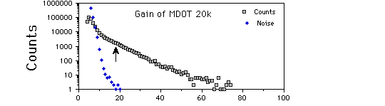
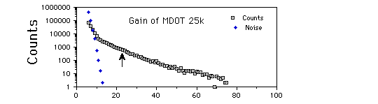
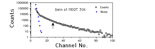 Figure 8: Photo electron spectra taken with MDOT at indicated values of
gain. The arrows represent the expected average pulse height
Figure 8: Photo electron spectra taken with MDOT at indicated values of
gain. The arrows represent the expected average pulse height
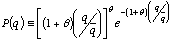
expected pulse height, which directly corresponds to the gain, is shown by an arrow and was obtained by dividing the Fe55 peak in an x-ray spectrum by 235 which is the expected number of electrons released by the 5.9keV x-rays. Polya7 fits to the spectra given by
display a disagreement between the expected gain and the Polya fitted gain. A
reduction of a factor of 3 is found and can be explained by the detector
geometry. The Polya fitted gain is smaller because the electrons are drifting
into the detector on the fringe of the drift field and arrive at the first row
of microdot cells. These cells have a smaller gain because they sit in the
fringe field of the detector. The calibration, using Fe55 x-rays, is
however obtained from the 99% of the detector that does not sit in the fringe
field and therefore has a higher gain. The distorted Polya fits to the pulse
height spectra show an increasing tail component, defined by the parameter
 ,
in the spectra at gains higher than 20k. It is clear from the results that by
connecting an amplifier to each string and by using modern integrated
electronics such as Microplex or Viking chips (ENC ~1000 electrons) that the
detector should be very efficient (>90%) for the detection of photons at
gains between 10 and 20k.
,
in the spectra at gains higher than 20k. It is clear from the results that by
connecting an amplifier to each string and by using modern integrated
electronics such as Microplex or Viking chips (ENC ~1000 electrons) that the
detector should be very efficient (>90%) for the detection of photons at
gains between 10 and 20k.
4.4 High Rate and Ageing Studies
The detectors response to high fluxes is crucial if considering using
such detectors for high rate applications. Figure 9 shows the behaviour of a 200
 pitch MDOT from the first batch to high fluxes of 8keV x-rays. The gain is
monitored at such high rates by using the current drawn from the anode dots. As
can be seen in the figure, the detector initially charges up by 15% but is
stable to further increases in rate. Ion implanted MSGCs using the same
technology showed a decrease in gain of 33% but were also stable to further
increase in rate8. This can be understood by considering the
interaction of the anode fields and the substrate fields. In the case of the
MSGC there is a mismatch between the natural logarithmic field given by the
geometry and the surface linear potential divider. Whereas in the case of the
MDOT there is better matching of the quadratic anode field and the quadratic
surface field potential divider. This match should be exact but is broken by
interaction between the substrate and the buried readout bus.
pitch MDOT from the first batch to high fluxes of 8keV x-rays. The gain is
monitored at such high rates by using the current drawn from the anode dots. As
can be seen in the figure, the detector initially charges up by 15% but is
stable to further increases in rate. Ion implanted MSGCs using the same
technology showed a decrease in gain of 33% but were also stable to further
increase in rate8. This can be understood by considering the
interaction of the anode fields and the substrate fields. In the case of the
MSGC there is a mismatch between the natural logarithmic field given by the
geometry and the surface linear potential divider. Whereas in the case of the
MDOT there is better matching of the quadratic anode field and the quadratic
surface field potential divider. This match should be exact but is broken by
interaction between the substrate and the buried readout bus.
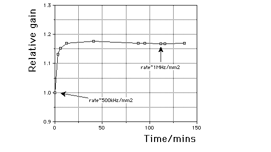 Figure 9: Response of batch 1 200 micron pitch MDOT structure to high
x-ray flux
Figure 9: Response of batch 1 200 micron pitch MDOT structure to high
x-ray flux
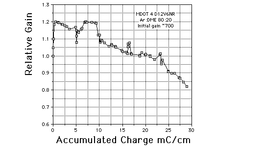 Figure 10: Ageing curve for 100 micron MDOT structure
Preliminary ageing measurements on a 100
 pitch MDOT from the first batch are given in figure 10, at a similar gain to
the tests performed with MSGCs and using a clean gas supply but with plastic
pipes and chamber materials. No decrease in energy resolution was observed up
to 25mC/cm. After irradiation the detector was scanned under a microscope and
no spark damage could be observed. However polymerised deposits had formed on
the electrodes where the x-ray beam was incident on the substrate. Attempts to
clean the deposits with propanol and acetone failed, but it should be possible
to clean and regenerate dirty detectors in a plasma photoresist asher as used
in the detector manufacture. This is only possible because the detector
contains no plastic insulation or passivation material unlike MSGC or MGAP
detectors.
pitch MDOT from the first batch are given in figure 10, at a similar gain to
the tests performed with MSGCs and using a clean gas supply but with plastic
pipes and chamber materials. No decrease in energy resolution was observed up
to 25mC/cm. After irradiation the detector was scanned under a microscope and
no spark damage could be observed. However polymerised deposits had formed on
the electrodes where the x-ray beam was incident on the substrate. Attempts to
clean the deposits with propanol and acetone failed, but it should be possible
to clean and regenerate dirty detectors in a plasma photoresist asher as used
in the detector manufacture. This is only possible because the detector
contains no plastic insulation or passivation material unlike MSGC or MGAP
detectors.
5 Pixel Readout
The silicon wafer on which the detectors are manufactured leads naturally to the possibility of integration of detector readout electronics. A very simple system has been proposed9 suitable for high rate x-ray images. Figure 11 shows this readout scheme, the individual dots are connected to an array of MOS transistors in the substrate which can be sequentially addressed and gated on to readout lines. The structure is similar to a dynamic RAM where the microdot anode-cathode capacity forms the capacitor of the RAM cell and therefore no integrated capacitors are necessary. The charge loss from the surface leakage channel through the implant is very slow taking a few thousand milliseconds, so the dots can be readout cyclically at a moderate rate, typically for a 20MHz clock each dot can be readout every 40 microseconds on a full 8 inch or 60 microseconds on a 12 inch wafer scale array. The device when addressed and readout in a parallel bussed fashion should allow very high pixel readout rates of typically 10 Giga pixels / second and is suitable for high yield wafer scale integration.
6 Possible Applications and Conclusions
The microdot gas avalanche detector is, without further development, suitable for x-ray imaging and particle tracking using the 2D capability. It has also been shown that the detector is capable of detecting single UV photons. The integration of the device on a silicon wafer leads to increased noise due to the large capacitance of the cathode.
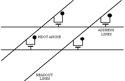
Figure 11: Schematic for proposed pixel readout
This renders the cathodes unsuitable for the detection of small pulses from
single photon avalanches. Simulation has shown that using a quartz rather than
silicon substrate can reduce the cathode capacity to a level where macroscopic
cathode pads (up to 20mm2) can be used. Such a detector should give
a high accuracy
 x,
x, y
y 2D detector suitable for UV RICH imaging when combined with a CsI coated
drift cathode.
2D detector suitable for UV RICH imaging when combined with a CsI coated
drift cathode.
Other advantages of the device are that no surface passivation is required and the 2D capability enables the detector to be used at a lower gain than in a 2D MSGC becauase of the increased ~85% anode-cathode pulse height ratio, compared to the ~50% achievable in an MSGC with backplane pickup.
References
[1] S.F.Biagi, T.J.Jones Nucl. Instr. and Meth. A361 (1995) 72-76.
[2] S.F.Biagi, J.Bordas, D.Duxbury, E.Gabathuler, T.J.Jones, S.Kiourkos. Nucl. Instr. and Meth. A366(1995) 76-78.
[3] Hughes Microelectronics Europa Ltd., Glenrothes, Scotland, UK.
[4] MAXWELL Electric field simulator, Ansoft Corporation.
[5] L.Alunni, R.Bouclier, G.Fara, Ch.Garabatos, G.Manzin, G.Million, L.Ropelewski, F.Sauli, L.Shektman, E.Daubie, O.Pingot, Yu.N.Pestov, L.Busso, S.Costa. Nucl. Instr. and Meth. A348 (1994) 344-350.
[6] S.F.Biagi, in preparation.
[7] J.Va'vra. Nucl. Instr. and Meth. A371 (1996) 33-56.
[8] S.F.Biagi, T.J.V.Bowcock, D.Duxbury, J.N.Jackson, T.J.Jones, S.Kiourkos. Nucl. Instr. and Meth. A367 (1995) 193-197.
[9] X-Image Ltd., 41 The Old Bath Road, Sonning, Berkshire RG4 0SY. Patent granted for medical imaging applications of pixel array readout