CEA/DSM/DAPNIA - CE Saclay
91191 Gif-sur-Yvette - France
Tel : (1) 6908 2229, Fax : (1) 6908 3024
E-mail: comby@hep.cea.fr
Abstract
The Ceramic Electron Multipliers (CEM) is a compact, robust, linear and fast multi-channel electron multiplier. The Multi Layer Ceramic Technique (MLCT) allows to build metallic dynodes inside a compact ceramic block. The activation of the metallic dynodes enhances their secondary electron emission (SEE). The CEM can be used in multi-channel photomultipliers, multi-channel light intensifiers, ion detection, spectroscopy, analysis of time of flight events, particle detection or Cherenkov imaging detectors.
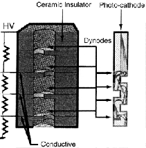
Fig. 1 - A principle of the CEM
CEM operating principle
The CEM operation principle is the same as a classical PM tube. A voltage divider establishes a voltage between metallic cavities. The metallic walls of the cavities are activated to enhance their secondary electron emission (SEE), which changes them to dynodes. Amplification of the dynode structure, coupled with a good electron transfer efficiency, creates a large amplification factor. Our dynode structure design inhibits the ion feed-back, which could damage a photocathode surface. The structure does not need the vacuum glass or metal envelope, or socket feed-through and allows to build very compact sensors.
CEM CHARACTERISTICS
Mechanical aspect
Raw ceramic sheets 0.05 to 0.5 mm thick are punched (to form cavities), painted with a conductive ink (to make conductive walls and conductive strips, in order to connect all inner elements to the external pads), packaged and fired to get a compact ceramic block. After that, the cavity walls are metalized by the chemical electro-plating technique to form metallic dynodes. The ceramic design enables a resistance to shocks and vibrations.
The CEM can be sized to a particular application. Up to 20 to 30 ceramic sheets can be packaged to build sophisticated structures. The standard dimensions of the MLCT components goes from 10 to 60 mm2. Larger sizes, up to 200 mm2, can be achieved, if necessary. CEM are produced by a High Technology mass production Industry. Such production allows uniformity, reproducibility, low cost of the components. After the metal coating of the cavities and the operating tests, these components are delivered ready-to-use by the ceramist.
Vacuum & Chemical aspect
The alumina and metals, together with a high firing temperature (~1500deg.C), produce very clean ceramic surfaces suitable for ultra high vacuum technique. In addition, a chemical stability of alumina preserves the physical properties in an alkali atmosphere.
Dynode electrical insulation
The resistivity of a 0.25 mm thick inter-dynode-stage is larger than 200
 at 200 Volts, allowing a very stable operation. A dynode surface activation
with cesium does not affect this stability.
at 200 Volts, allowing a very stable operation. A dynode surface activation
with cesium does not affect this stability.
Dynode activation
The dynode activation is achieved by a chemical process involving alkali metals plated on the electrode, and cesium vapor, creating a very thin and reactive layer with low work function. The secondary emission can be enhanced by a factor 10 to 20 depending on the nature of the elements and the preparation of the metallic surfaces. Several ways exist so that: each manufacturer proceeds with its own technique to produce efficient emitting dynodes. In our study, a SbCs layer was formed on the dynodes-cavities from electro-plated antimony. We achieved a dynode gain of 6-7 per stage voltage of 200 Volts. We obtained a total gain of ~1.5x10³ using six stages. A very stable operation was observed. A larger number of the dynodes can produce a multiplication factor up to ~106.
 Fig. 2 - Dependence of a transit time, rise time and a jitter on the dynode
voltage.
Dynamic characteristics
We measured a rise time of 1.6 ns for a dynode voltage of a 180 Volts, using a laser flashes with a 900 ps duration. When the dynode voltage increased from 60 to 200 Volts, the transit time decreased from 7 to 4.5 ns, and the corresponding jitter decreased from 150 to 100 ps.
No modification of the electron multiplication was observed during the double-pulse tests when the delay between flashes decreased to zero. The absence of a recovery time proves that a continuous pixel sensitivity and a gain independent of the flash delay.
Linearity
No saturation affects were detected in the output pulses, up to a charge of 250 pC at a dynode voltage of 180 V .
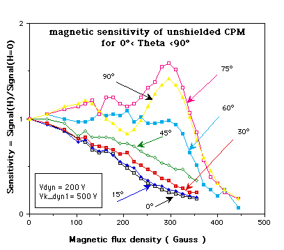
Fig.3 Sensitivity of the CEM output on the magnetic field.
Operation in magnetic field
The small dimension of the cavities and their compact structure enables to work in a magnetic field up to 200 Gauss for CEM channel axis parallel to field H, and up to 360 Gauss when perpendicular to field. A symmetrical arrangement of the dynodes preserves the CEM output signal whatever is a Phi rotation around the Anode/Cathode axis from 0 to 360deg..
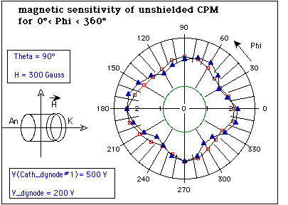
Fig.4 Sensitivity of the CEM output on the magnetic field.
CEM Applications
The manufacture of sealed detectors (assembling, activation, sealing) necessitates the use of the transfer method in order to preserve the high quality of the activation.
The CEMs included in open setups require a special dynode coating to assume convenient secondary electron emission level and to tolerate the break-down of the vacuum.
Equiping the CEM with a glass window bearing the photocathode and a ceramic socket including the output pixel pads, produces compact multi-pixel ceramic photomultiplier.
Replacing in a previous application, the output socket by a glass bearing phosphorescent pads, produces a multi-pixel light intensifier.
Included in the detection group of a mass spectrometer, the CEM allows to make a dynamic imagery of the ion detection.
CEM can be also adapted:
- to build ultra high vacuum sensors
- to enhance the electronic flux of pulsed photocathode injectors
- to form multi-lens electrostatic structure to guide and to distribute electron flux
____________________________
REFERENCES
( 1 ) G. Comby and F. Lehar, - A ceramic multi-channel electron multiplier for a new multi- channel PM-, presented at the Int. Workshop on Heavy Scintillators for Scientific and Industrial Applications, Chamonix, 1992.
( 2 ) G. Comby, F. Lehar, E. Chassaing, G. Lorthioir, - Status of the ceramic multichannel PM tube -, Nucl. Instr. and Meth. A 343 (1994 ) 263-267.
( 3 ) G. Comby, M. Karolak, Y. Piret, J.P. Mouly et al, Performances of multi-channel ceramic
photomultiplier -, Int. conference on Inorganic Scintillators and their Applications, DELFT University of Technology, the Netherlands, 1995.